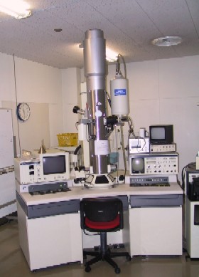
1) Transmission Electron Microscopy (TEM) (Room 1)
Ultrastructures of biological or non-biological specimens can be obtained by magnifying the ultrathin sections by 100 to 1,000,000 times. The resolution limit for lattice image is 1.44 A and that for structure image is 2.1 A. Five steps of accelerating voltages from 75 kV to 200 kV make it possible to observe the sections of a wide range of thickness. Since the H-8100 is computer-controlled, any beginner can get satisfactory data instantly. The biological specimens are usually observed after being stained with various metal solutions. However, the H-8100 can observe a bright or a dark field image of non-stained specimens with a scanning-transmission (STEM) mode. It is also possible to make a stereo pair of photographs by changing the tilt angle of semi-ultrathin sections. The ultramicrotome (in Room 2) and equipment for freeze-etching and freeze-fracture techniques are also available in the Center.
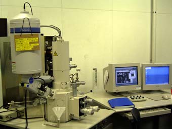
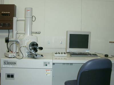
2) Scanning Electron Microscopy (SEM) (Room 1)
The surface of tissues, cells, bacteria, viruses, and non-biological materials whose thickness are up to 0.5 mm can be observed with a resolution of 3 nm. A critical point drying apparatus (in Room 5) and an ion coating apparatus (in Room 5) for the sample preparation are available in the Center.
3) Electron Diffraction (ED) (Room 1)
From the diffraction pattern with selected area diffraction mode, the crystallographic structure of crystalline materials can be analyzed. The H-8100 has a computer-controlled lens that provides the best correlation of selected area image and diffraction pattern for all magnifications. |
4) Energy Dispersive X-ray Analysis (EDX) (Room 1)
An elemental microanalysis can be achieved by detecting a specific X-ray energy emitted from specimens on application of the electron beam. Point, line, and area analyses can be carried out by viewing the SEM and TEM images of the specimens. The obtained data can be analyzed qualitatively and quantitatively with a Kevex DELTA software FLAME. Various kinds of expression for digital data imaging are possible with this system, for example, the STEM image can be decorated by elemental mapping.
5) Electron Energy Loss Spectroscopy (EELS) (Room 1)
The H-8100 is capable of performing electron energy loss spectroscopy either in TEM or in SEM mode. The composing elements, mostly light ones like B, C, N and O of specimens can be analyzed by measuring the energy loss of electrons passing through the specimens. The resolution is 4 eV.
6) Dimple Grinder (GATAN Model 656/3) (Room 1)
?Dimple grinder is an instrument used for grinding circular dimples of spherical profile in the surface of materials such as ceramics and semiconductors. The fundamental application is to prepare the specimens for TEM observation. This technique is normally used for pretreatment of ion milling. The operator can carefully produce a specimen with the thickness less than 5 mm. However, in most cases, a final thickness between 20 and 50 mm is normally obtained.
7) Ion Milling (GATAN DuoMill Model 600) (Room 5)
The DuoMill is a machine which can "mill" the specimens such as ceramics and semiconductors for TEM observation. Ion milling involves directing a several-keV beam of argon ions at both sides of a specimen. As the ions strike the specimen, the surface atoms are sputtered out, which leads to thin the specimen. GATAN DuoMill has two chambers which contain all the facilities for independent ion-thinning of two specimens. |