
Thin film silicon solar cells have advantages such as production with lesser sources and easiness of wide area production with low cost. Thin film silicon solar cells have come into wide use as crystalline silicon solar cells. In order to come into wider use, however, it is necessary to solve many remained problems and improve the efficiency.
In thin film silicon solar cells research and development group, we have been engaged in the research and development of silicon based solar cells toward realization of high efficiency and wider use of silicon based thin film solar cells. Our theme of research and development are mainly deposition and evaluation of silicon based thin films and development of transparent conductive oxide, characteristic evaluation technique with nano-meter resolution, and hetero-junction silicon based thin film solar cells as follows.
‡@Deposition and evaluation of silicon based thin films
Amorphous and microcrystalline materials such as
amorphous silicon, microcrystalline silicon, amorphous silicon carbon are used
in silicon based thin
film solar cells. We have deposited amorphous and microcrystalline silicon
based films by plasma enhance CVD and hot-wire CVD. We have also evaluated the structural,
electric, and optical properties. Based on these results, we have struggled to
improve the quality of silicon based thin films by clarifying its process
condition correlation and the characteristic of each material. Furthermore, we have
also developed novel thin films such as silicon with nano-ball structure and
microcrystalline silicon carbide in order to make new breakthrough.
‡ADevelopment of transparent conductive oxide
In silicon thin film solar cells, transparent conductive oxide (TCO) are generally used as electrodes. The technology related to TCO is one of key technology to improve the efficiency of silicon thin film solar cells. At present, TCO such as indium tin oxide, tin oxide, and zinc oxide are used. In the deposition of microcrystalline and nanocrystalline semiconductors, however, there is a problem that optical transmittance of TCO decreases due to deoxidization by hydrogen radicals. Since large density of hydrogen radical is needed in the deposition of microcrystalline and nanocrystalline semiconductors. To solve this problem, we propose to use titanium oxide, which has high durability against hydrogen radicals, as protection film and the development is moving on. In addition, use of poisonous element and rare element is problem in materials. To solve this problem, we have also engaged in the development new process of TCO and novel TCO materials.
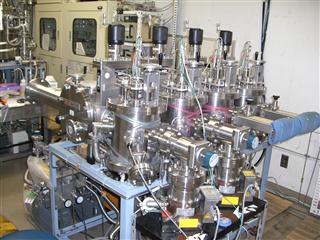
Deposition system for silicon based thin films &
solar cells
Silicon based thin film solar cells are produced by pilling few semiconductor
layers. This system has 4 different reaction chambers and transfer rooms,
able to produce different thin film in each chamber, and able to transfer
between each chamber without exposure to air.
‡BDevelopment of evaluation technique
In silicon based thin film solar cells, microcrystalline materials such as microcrystalline silicon are used. microcrystalline material is composed of micro size crystal and amorphous. In this kind of material, it is important to understand its characteristic within small domain in order to improve the quality. And also, the efficiency of thin film solar cells using microcrystalline material would be affected by its small domain characteristic. The evaluation technique used for properties of materials and thin film solar cell performance until now is macroscopic one, but unable to be used for evaluation within small domain.
By using scanning probe microscope technique with resolution to observe atom image, therefore, we are going on the development of evaluation technique which can evaluate the properties of microcrystalline materials and the performance of thin film solar cells. As properties of microcrystalline materials and characteristic of thin film solar cells using this technique, improvement of quality of microcrystalline materials and efficiency of thin film solar cells based on the evaluated results.
Amorphous and microcrystalline silicon based thin film solar cells are in silicon based thin film solar cells. We have deposited amorphous and microcrystalline silicon based thin film solar cells and evaluated their evaluation. By improvement of quality of thin films, technology related to solar cells such as TCO, and structure of solar cells including junction characteristics based on results obtained though above researches and developments, we have been engaged in the improvement of efficiency of amorphous and microcrystalline silicon based thin film solar cells. Multi-junction thin film solar cell can convert light power with wider wavelength region to electric power by combination of solar cells with sensitivity of different wavelength region and recently its development is going on. Therefore, we are also developing silicon based multi-junction thin film solar cells. Furthermore, we have been engaged in the development of thin film solar cells using novel materials such as silicon with nano-ball structure.
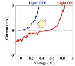
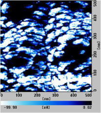
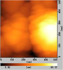
Surface
morphology and current image of silicon based thin film solar cell
By
using evaluation technique which we are developing, photo-current image (upper-right
figure) and surface morphology (upper-left figure) in the same area of active
solar cell under light irradiation can be observed at the same time. From these
results, we can understand the relation between photo-current and surface
morphology. Here, the surface height and the photo-current in the brighter
regions are higher and larger, respectively. And also current-voltage characteristics
under dark and lit irradiated conditions can be observed.
For photovoltaic films of the next generations solar cells, development of novel materials are necessary with a variation and a controllability of their band gaps. In our group, we focused on a material, called silicon clathrate, which is one of silicon allotropes and have cage structures composed with Si atoms. One of key properties of the material is the wider direct band gaps lying in the range from 1.9 to 2.0 eV. However, understandings of their synthesis mechanisms and their characteristics are still not fully conducted even in the world. Recently, we carried out the characterizations of the Si clathrate as a parallel works of optimization works of the synthesis conditions. A photosensitivity appeared from a Si clathrate pellet which is the first practical result suggesting to the possibility for applications to the solar cells. Furthermore, this material is expected to tandem solar cells based on only group IV materials.
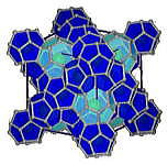
Schematic image of silicon clathrate lattice (Type
II)
A crystal lattice of silicon clathrate is formed by the combinations of cage structures which are composed by silicon atoms. Each cage generally has a metal atom inside which is called a guest atom. The electrical characteristics of silicon clathrate vary from metallic to semiconducting as the occupation ratio of guest atoms inside cages changes.